

Deep Dive: INTC Valuation; Foundry Pipeline & Customer Predictions
Aria's Valuation Projection's for Paid Subscribers

As you know, at Aria Research, Intel is one of our highest-conviction companies, so it is only appropriate that we provide an in-depth description of Intel’s foundry pipeline, along with our view of its stock valuation through 2030.
We are going to upload the same Excel File we used to model Intel’s valuation for Paid Subscribers. The Excel file we created allows you to “plug and play” with numbers and scenarios, so even YOU could make your own valuations. That being said, let’s embark on the “Intel model”.
Pillar 1: Assumptions
With our valuation model, there are some assumptions we have made in order to forecast EPS. We purposely left out any incremental AI accelerator revenue over the next 5 years, as they currently hold negligble market share in this space. We assumed as well that Intel will maintain 25% market share in server CPU’s, with a TAM of $170 billion. Anything related to the consumer market is priced into the base EPS of $6.24. This articles purpose is to ONLY model the Foundry pipeline through 2030…
Source: Aria Research
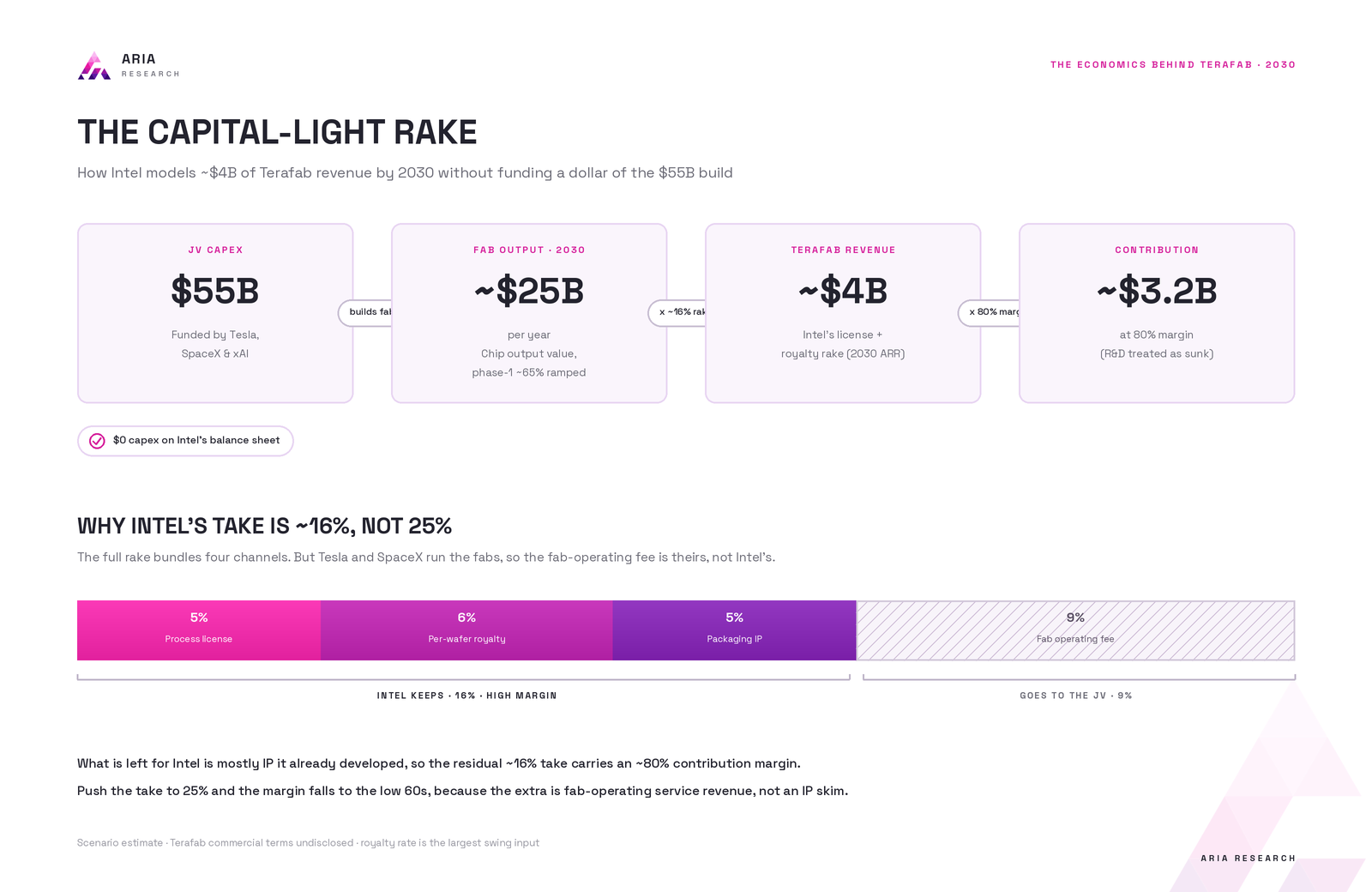
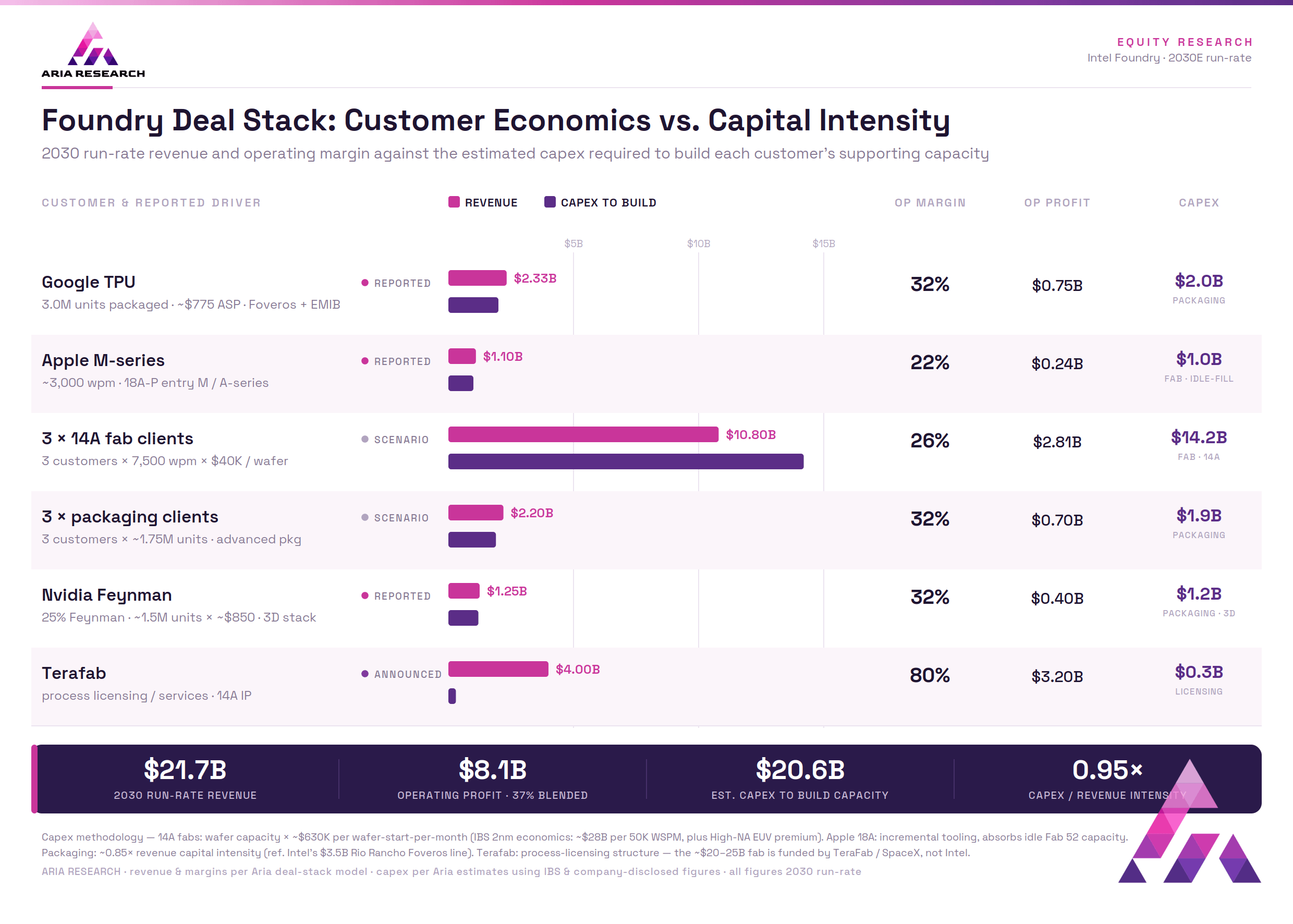
The Tera-Fab Deal:
The Tera-Fab project is a $55B joint venture between Tesla, SpaceX, and xAI, unveiled by Musk in late March 2026.
(The $55 billion is the phase-1 budget per SpaceX S-1, with full $119B scale occurring in the mid-2030s, and targeting 1 terawatt of compute per year)
Essentially, Intel would be licensing their fabrication IP and advanced packaging technology for Tesla automotive Chips and Optimus Chips, with the first chips in late 2027 and full-scale production in 2028. Intel signed on April 7, 2026, as the primary foundry partner, contributing the 14A process, advanced packaging, and design/fab expertise (Tesla selected Intel’s 14A for its Terafab chips, and SpaceX is also planning to use it).
This deal is structured so that the $55+ billion used to fund the project comes out of SpaceX/Tesla’s wallet. There is no debt affecting Intel from this agreement. Essentially, Intel is offering their expertise in chip-fabrication/packaging while maintaining 80% margins on their revenue share from Tera-Fab. By 2030, after initial ramping, we model this joint venture to have an ARR of around $4 billion. We believe demand for chips will keep Tera-Fab capacity constrained, allowing Intel to maintain pricing power.
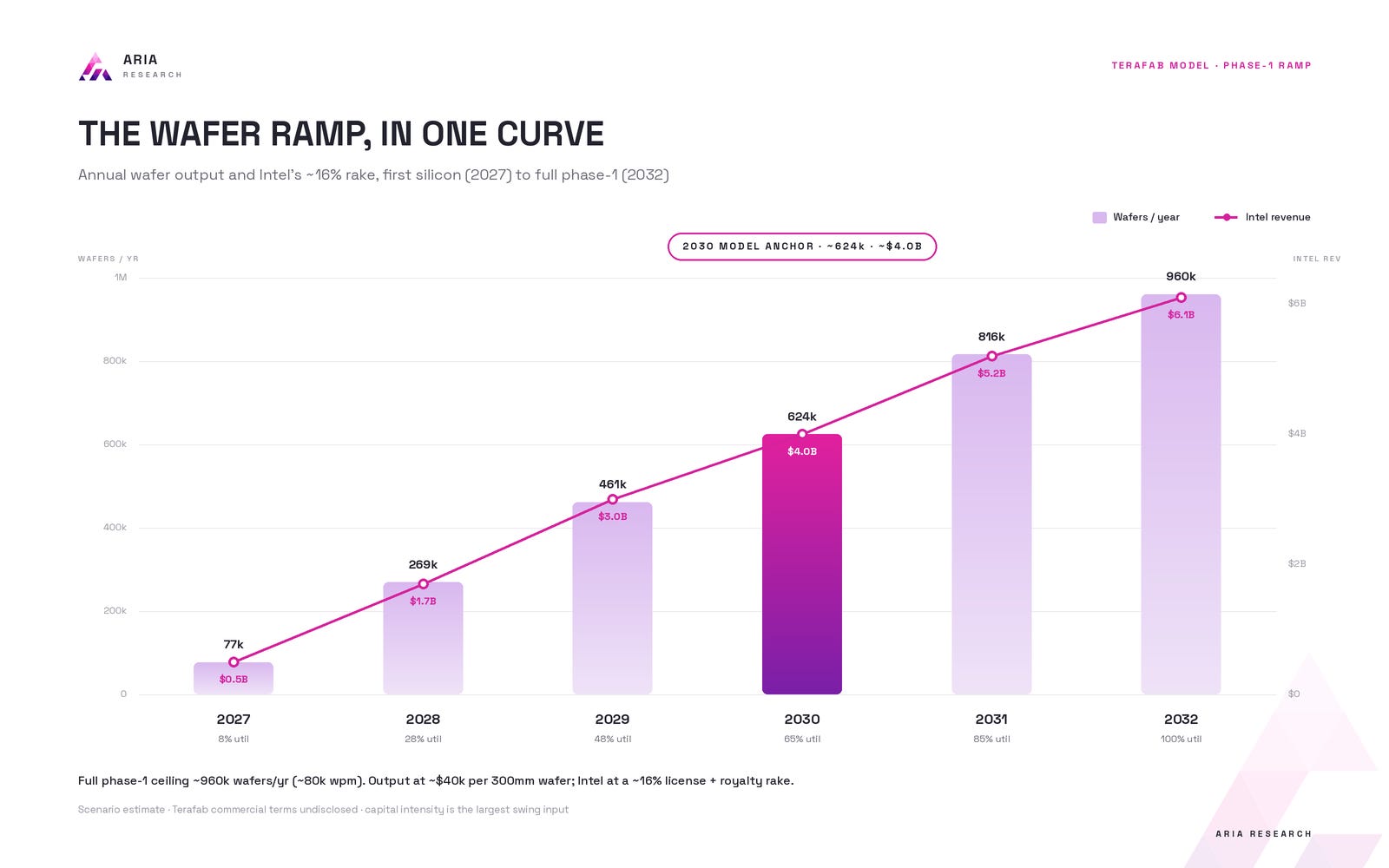
The Economics Behind Tera-Fab:
Total capex spend by 2030 is $55 billion; modelling a fab the size of $55 billion at full ramp can produce up to 52,000 WPM (wafers per month) at 65% ramp capacity; we also project full Phase-1 will be fully ramped and capacity utilized by 2032, with a total projected production capacity of 80,000 WPM, or 960,000 WPY. By 2030 using the base revenue split at 16% allocated to Intel, this leaves them with $4 billion in revenue off of a $25 billion output. There have been specualtions about the revenue split being higher than 13%-16% (around 25%), but this cannot be true as Tesla/SpaceX will operate the FABs themsevles, and Intel would be liscencing their IP. Thus the reason why they can garner 80%-90% margins, but only a maximum of 16% revenue split.
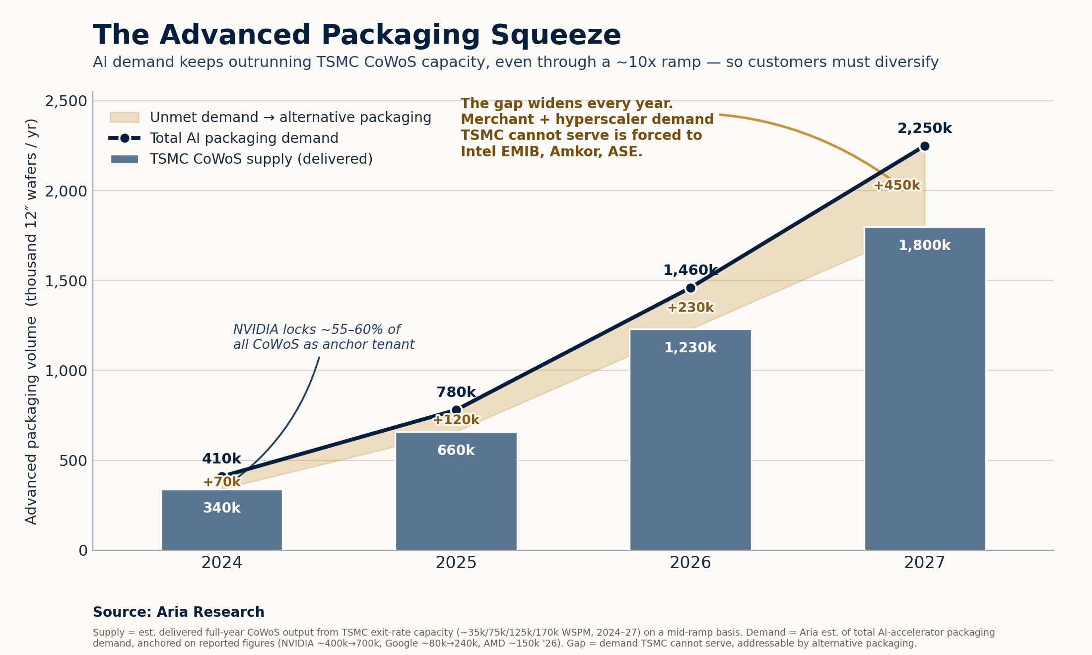
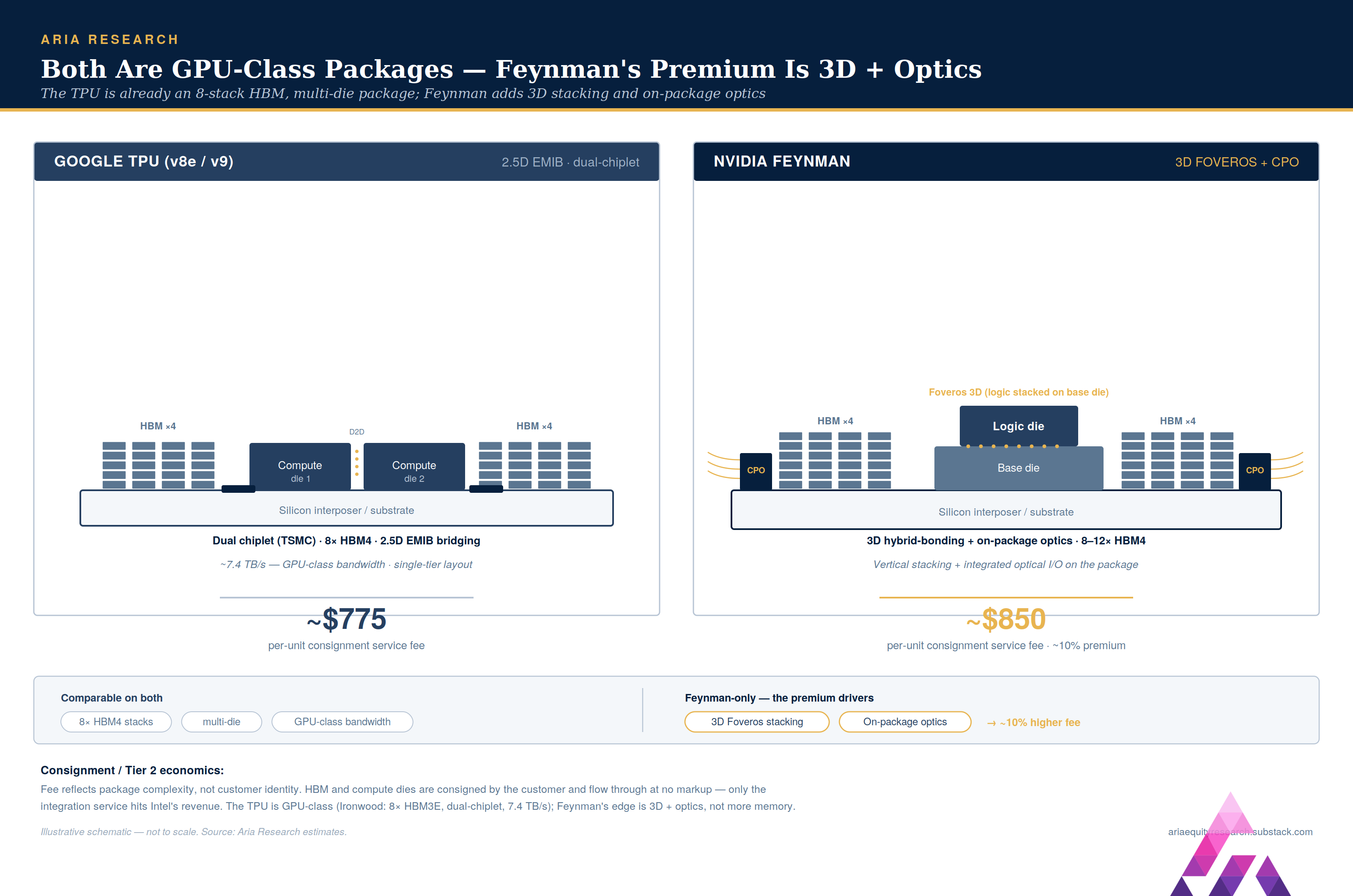
Google TPU Packaging:
The Google TPU deal involves the advanced packaging of 3 million TPU’s for 2028. This will cover roughly half of Google’s TPU supply, with production beginning in 2027. (6 million) As reported, this deal is strictly for advanced packaging, although various sources have stated that it involves fabrication as well. We modelled this strictly for packaging. (If the deal includes chip-fab, the ARR can easily stretch upwards of $5 billion, on a 26% combined margin.)
Using advanced packaging and TPU pricing data, we model this to have an ARR of $2.325 billion, on a 32% operating margin. We landed on these numbers through standard packaging and TPU economics. We predict Intel will charge 70% of TSMC’s CoWoS pricing, as they’ve stated they will offer customers a price-efficiency advantage. (Intel charging roughly $775/unit for 3 million TPU’s equates to $2.325 billion in revenue.) The Google deal was the first large-scale customer Intel landed for its advanced packaging services. This not only benefits Intel by restoring external foundry credibility but also benefits Google by de-risking its reliance on TSMC’s CoWoS and diversifying its supply chain. We thoroughly believe that this will spark more tech giants to adopt Intel’s EMIB technology, given the sheer capacity constraint of the packaging market.
Use this chart below as a reference for TSMC CoWoS bottleneck…
Source: Aria Research
Nvidia Feynman:
Rumours have been circulating that Nvidia is showing interest in Intel’s EMIB technology. The rumours indicate that 75% of Feynman would be allocated to TSMC and their CoWoS technology, whereas the remaining 25% would go to Intel Foundry. Using the 25% number (and also predicting the volume for Feynman), we can allocate a volume of 1.25-1.75 million units.
Using $850/unit and the expected volume, we arrive at a revenue range of $1.04-$1.46 billion. NVIDIA’s higher-end GPU would call for higher pricing than other chips simply because it has a higher bandwidth-bound flagship with next-generation HBM.
This results in Intel using its Foveros 3D die-stacking and co-packaged optics, resulting in a physically larger package than the average chip. Packaging a next-generation chip like Feynman has more bond sites and more bridges and requires 3D hybrid bonding instead of 2.5D. This will lead to more assembly/test work and more yield risk, resulting in a higher service fee for Nvidia.
Apple Fabrication Deal:
The next reported deal is between Intel and Apple. The reporting suggests that Intel will manufacture legacy Apple chips on its 18A process node, with estimates of 15 to 20 million M-series chips a year allocated to Intel, with major ramping beginning in 2027. More recent reporting has Apple showing interest in Intel’s 18A-P node for an entry-level MacBook chip, while also evaluating the 14A process node for more advanced chips. We modelled this to have an ARR of between $1.0-1.2 billion for the entry-level chips. For Apple, this is the beginning of breaking their near “full dependence” on TSMC for fabrication.
This could approximately provide Intel with $1.1 billion on a 22% operating margin. The margin sits below the packaging deal by 10 percentage points, because this is wafer-side work, where costs allocated to process-nodes are much higher. Due to the “crown jewel” of foundry services sitting within chip fabrication, the true value of this deal provides Intel with external fabrication credibility. This validation is even more important, given how supply-constrained TSMC actually is.
For reference, TSMC’s 2nm node is already completely booked through 2028, while Apple currently holds just under 50% of the demand. In layman’s terms, there is no “extra slack” left for Apple to grow their 2nm footprint with TSMC. Currently, TSMC’s 2nm capacity has 78-104-week lead times, pushing new orders into 2028. Even at 100,000 WPM, N2 capacity still remains lower than the combined demand from customers. This can make a strong case for Apple to use Intel’s more advanced nodes in the future for chips such as the A21. CEO Tim Cook specifically stated that they are unable to ramp up supply to meet demand for their advanced chips. Which, in theory, could open up a foundry pipeline between Apple’s advanced chips and IFS. If Intel were to win the A21 chip with average volumes of 40-60 million per year, this alone could supply them with an extra $3.0-$4.9 billion in ARR.
Although this is a possibility, we are purposefully leaving this out of our model as Intel hasn’t fully solidified their advanced nodes as “achieving profitable margins” just yet. Although we believe that the 14A node will be deployed faster than projected (currently 50% yield), the reporting indicates that the A21 will be on TSMC’s N2 node, which makes a lot of sense, given that Apple is a priority customer for TSMC. Overall, at full ramp, the entry-level M-series chips would have an annual revenue run rate of $1.1 billion.
Advanced Packaging Customers:
For Intel, we predict 3 additional advanced packaging customer commitments by 2030, alongside Google and Feynman. We predict the three customers will have an ARR of $2.2 billion. For argument’s sake, we assumed that the customer volume wouldn’t be the same size as Google’s large-scale 3 million orders; we instead modelled it to be around 1.5-2.0 million units per customer.
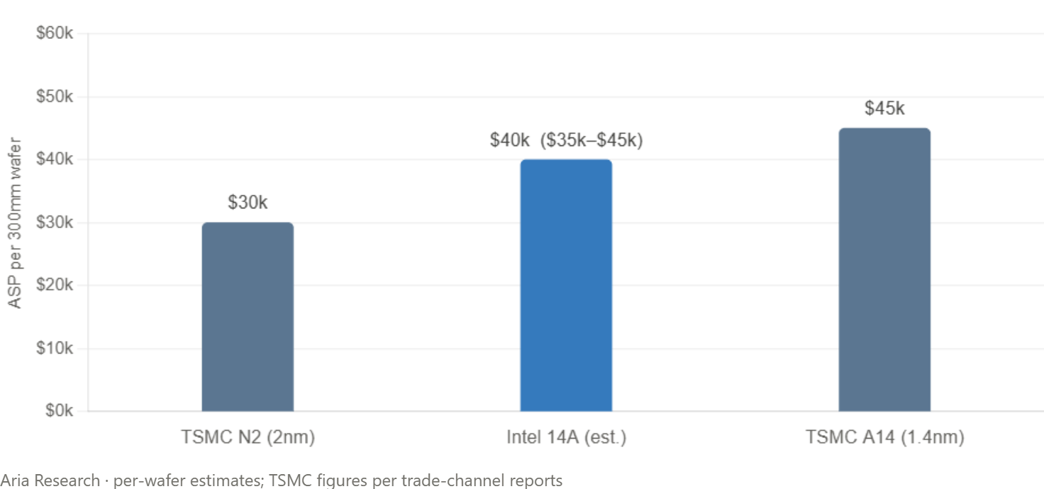
Large-Scale 14A Customer
In our model, we forecast 3 large-scale customer commitments to Intel’s 14A process node. The revenue per customer sits at $3.6 billion, resulting in a total of $10.8 billion. We modelled this number through thorough estimations of the Wafer ASP for a 1.4nm class-node, along with potential volumes that could be reflective of a “large-scale customer.” Our thesis for Intel’s foundry doesn’t imply the takeover of TSMC on a large scale; it implies companies like Apple utilizing both foundry services as a hedge against a bottleneck within the market. In terms of wafer demand per month, we estimate each customer would command 7,500 wafers per month, roughly, valued at $40,000/wafer. TSMC expects to charge $45,000 per wafer on their A14 1.4nm node. CFO Zisner specifically stated that Intel’s 14A node will have a cost-efficiency advantage while remaining competitively priced. Overall, we believe the $35,000-$45,000 range suffices.
Source: Aria Research
We personally believe that 3 large-scale customer commitments through 2030 are on the more conservative side, and this is done so purposefully to show you the upside potential Intel truly has. Multiple companies have reportedly shown interest in Intel’s 14A process node. Intel has confirmed a partnership with Elon Musk on the Terafab project, while also hinting at several more customers. CEO Tan has also specified that they will not mention the names of any potential customers until they agree to do so. 14A design commitments are expected to start landing in the second half of 2026 and run into the first half of 2027.
The reason these deals have a structural aspect as opposed to a speculative one comes down to the capacity constraint we’ve been preaching about. TSMC’s leading-edge node is effectively sold out, with N2 fully booked. AI buyers are currently trying to outbid one another for allocation. Even Apple, TSMC’s priority customer for over a decade, has dropped below 50% of N2 capacity for the first time as Nvidia and the hyperscalers soak up the node. This forces companies, like Apple, to diversify their supply chain in order to scale supply to meet the red-hot demand. If the demand for XPU’s continue to accelerate (as the data suggests), then large-scale companies that need to increase supply have no other choice but to allocate wafers to Intel’s 14A.
Source: Aria Research
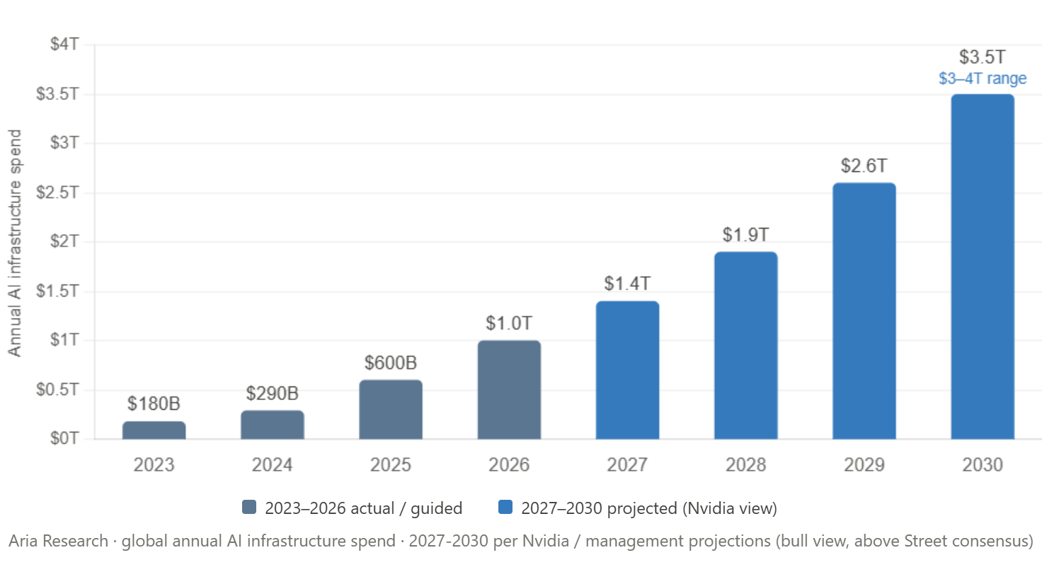
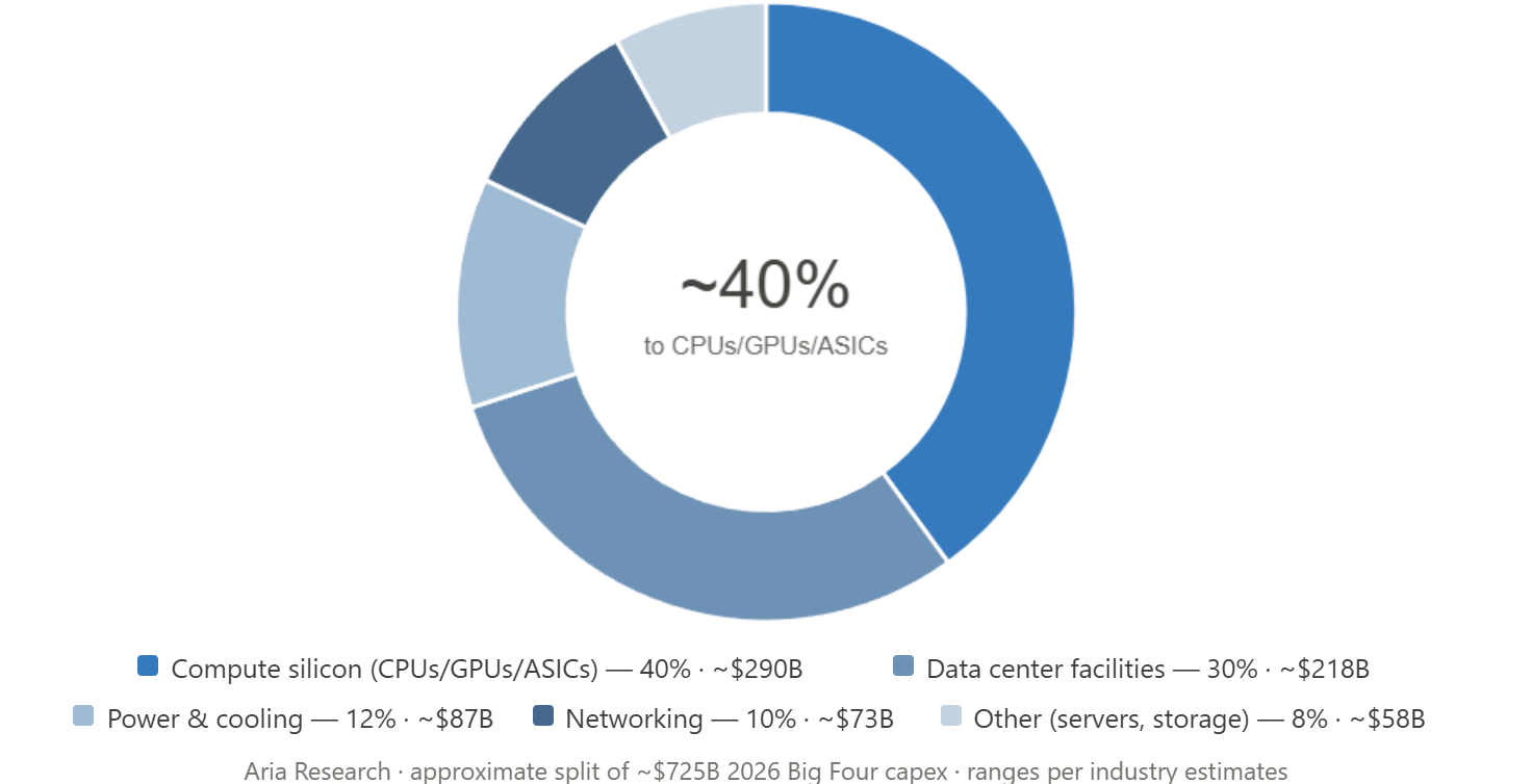
Above are estimations for overall capex allocated to the AI buildout through 2030. Jensen Huang successfully called for $1 trillion in capex by 2026 in the year 2023, and is now predicting 3-4 trillion alone by the end of the decade. Around 40% of all capex is invested into compute, meaning the amount of XPU’s that need to get fabricated will increase alongside Capex.
The Debt Structure:
Inside of the base EPS estimate, we have already included the debt that Intel has incurred PREVIOUSLY in order to buildout their foundry services. The 6% cost of debt comes from the marginal or new-issue rate; in other words, “what Intel would pay to borrow fresh money today at BBB, or a negative outlook.”
Share Dillution:
Before we begin, let’s address the share dillution: Our model assumes that through 2030, Intel will have added roughly 400 million shares to the market to raise capital. In the year 2025, Intel had utilized this method, and the equity structure is as follows…
US Government Stake: 433.3M x $20.47 = $8.9 billion
NVIDIA: 214.8M x $23.28 = $5.0 billion
SoftBank: 87M x $23.00 = $2.0 billion
TOTAL: 735M Shares for 15.9 Billion Raised
We believe it makes the most sense for Intel to lean heavily on share issuance, as their stock price has received an immense re-rating. In 2025, their share price was hovering around $20- $25 per share, whereas today it’s 5x that level. This means that for less overall dillution they can raise more money, making equity the far cheaper option than debt. If Intel decided to go to the bond market and rely heavily on debt, it would only add costs and harm its balance sheet.
If Intel decides to issue 400 million shares through 2030 (80 million shares per year) at around $100-$110 per share, it could raise $40-$44 billion. This amount of money alone allows them to fully fund the external foundry capacity needed to satisfy our model…
It would cost roughly $20.6 billion to fund the “Aria-foundry model.” Unfortunately, Intel can’t just build a fab that can output 22,500 WPM of leading-edge capacity; Intel must build the whole 40- 50 K WPM fab. (Fab 52 as a reference is 40,000 WPM) The total “funding job” required to build out both fab/packaging facilities at comparable wafer outputs would cost around 30-40 billion dollars. Given this figure, share issuance alone can cover the entire cost. A large caveat that we must cover is the 48D tax credit, from the Big Beautiful Bill…
48D Tax Credit:
The mechanism of the credit allows for a 35% reduction in Capex for qualifying fabs and machinery. The refundable nature of the credit is what makes it very material to Intel. Intel can elect to take the credit as a direct cash payment from Treasury, which means they collect the money even while Intel Foundry is still operating at a loss on paper. A normal tax break is worthless to a company that isn’t paying tax. This one writes a cheque regardless. Essentially, the United States government is co-funding a fab, in cash, with no shares issued, no debt added, and no profit splits. It’s the single most useful funding strategy of their lifetime and puts Intel right in the driver’s seat. The only catch for the credit is that it is only applicable to fabs that break ground before December 31st, 2026, meaning any fab starting construction in 2027 or later cannot reap the tax credit rewards.
In theory, Intel doesn’t even need to raise any debt to fund their foundry, since equity and the 48D Tax Credit are by far the much cheaper options. For our model, we actually assume no new incremental debt will be taken on by Intel through 2030.
Incremental Debt:
So why do we model zero incremental debt through 2030? Because there is nothing left that would require extra debt to fund. The 48D Tax Credit returns 35% of the buildout in cash, cheap equity covers most of the funding required for fabs, and customer pre-payments cover the rest. Debt is the most expensive capital Intel can raise, roughly 6% against an equity cost near 1.2-1.5% and a 48D credit that costs nothing, so a rational management team reaches for it last, and in our model, we believe they never have to.
This doesn’t mean that Intel stops issuing bonds. It will keep rolling over its existing maturities, but refinancing them isn’t incremental debt added to the balance sheet, and the ~$46 billion already pencilled into the base EPS won’t increase any further. If anything, the bigger question our model raises isn’t whether Intel needs debt; it’s whether it even needs all the equity we’ve pencilled in (as cash flow turns positive for the external foundry business, the funding sources start to overlap). Debt only re-enters in our downside case, where weaker cash flows and a pullback in the stock reopen the door to debt over equity. In the base case, it stays at zero, and the balance sheet quietly heals. The bull case is less share dillution, with the implication that the stock continues to surge. (A bull case could warrant 200-300 million shares as opposed to our 400 million model.)
The 1.2-1.5% number represents the earnings yield. , and then using the current Foward PE multiple of 65-85x gives us an earnings yield of 1.2-1.5%. We decided to use the earnings yield over CAPM since CAPM is built specifically for discounting future cash flows and valuing companies. What it doesn’t do well is answer the question of “should I fund this fab with stock issuance or bonds this year.” Comparing that to the established 6%, equity is the much cheaper option to build out their foundry business. Just to reiterate, we used the earnings yield because the equity-or-borrow decision hinges on earnings given up per dollar raised, not on investors required return.
How Much Higher Can Intel Stock Go?
From our homemade valuation model, we have a generous price target set for Intel.
The following images showcase an in-depth analysis of the whole foundry pipeline, along with the incremental EPS each deal provides, EPS before and after financing, and the 2030 “Intel value,” with a 12-month price target.
